Describe this circuit
Components: Input pin A; Input pin B; XOR Gate 1; AND Gate 1; Output pin S; Output pin C.
- Input pin A connects to XOR Gate 1, AND Gate 1 (net A).
- Input pin B connects to XOR Gate 1, AND Gate 1 (net B).
- XOR Gate 1 connects to Output pin S (net S).
- AND Gate 1 connects to Output pin C (net C).
Before you start
If you do not have it yet, download Logisim safely. If it will not open, see Logisim will not open. Not sure which version? See Logisim vs Logisim-evolution.
A 60-second tour of the window
The Logisim-evolution 5.0.0 window with a half adder open: the menu bar (File, Edit, Project, Simulate, FPGA, Window, Help), the Design and Simulate tabs, the component tree with libraries, the toolbar with Poke, Edit and Text tools, pins, gates and flip-flops, and the canvas with an XOR gate and an AND gate.
- Menu bar: File, Edit, Project, Simulate, FPGA, Window, Help.
- Design and Simulate tabs above the component tree.
- Component tree: the libraries Wiring, Gates, Plexers, Arithmetic, Floating Point Arithmetic, Memory and Input/Output hold the parts you can place.
- Toolbar: Poke (the hand), Edit (the arrow), Text, then input and output pins, the basic gates, a flip-flop and a register.
- Canvas with a dot grid: this is where you draw. The Properties panel under the tree shows the settings of whatever is selected.
The full tour is on Interface and shortcuts.
Build a half adder
A half adder adds two bits. The sum is A XOR B and the carry is A AND B.
Name your circuit and save it first
Choose File, Save As… (CtrlShiftS⌘⇧S (⌘⇧S on macOS)) and name it
half-adder.circ. Saving first means you never lose work to a crash. Logisim-evolution also has autosave, but save by hand anyway.Check: A file named half-adder.circ exists.
Place two input pins
Click the Input pin tool in the toolbar, then click the canvas twice, one pin above the other. Give them labels now: select a pin with the Edit tool and type
AandBin the Label field of the Properties panel.Check: Two input pins are on the canvas.
Place an XOR gate and an AND gate
Click the XOR Gate tool in the toolbar and click the canvas. Do the same with the AND Gate tool, below the first. Both have two inputs by default; the Number of Inputs attribute changes that later (see Logic gates). The small dots on a gate are its ports: wires connect there.
Check: An XOR gate and an AND gate are on the canvas, to the right of the pins.
Place two output pins
Click the Output pin tool and click the canvas twice. Label them
Sfor sum andCfor carry.Check: Two output pins are to the right of the gates, labelled S and C.
Wire it
Drag from a port to another port. A wire is straight, so a bend needs two drags. Wire A and B each to one input of the XOR and one input of the AND; wire the XOR output to S and the AND output to C. A dot appears where three wires meet.
Check: Every pin and gate port is joined by a wire.
Test it with the Poke tool
Click the hand icon (the Poke tool), then click input A. In our test one click on A changed it from 0 to 1, and S followed at once. Logisim draws a magenta ring where you clicked.
LAB lab-lnx · Linux lab5.0.02026-11-11The half adder after one click on input A with the Poke tool: A shows 1, the sum output S shows 1 and the carry output C shows 0. A magenta ring marks the click.
One Poke click on A: A = 1, S = 1, C = 0 (F83).lab-lnx-le500-tutorial-poke-a-01 Click B as well: S goes back to 0 and C becomes 1.
LAB lab-lnx · Linux lab5.0.02026-11-11Both inputs 1: S = 0, C = 1 (F83).lab-lnx-le500-tutorial-poke-ab-01 The four rows to check. Tick each one as you see it. # A B S C 0 0 0 0 0 1 1 0 1 0 1 0 1 1 0 1 Check each row0 / 4 doneCheck: The outputs match the four rows below.
Check with the automatic truth table
Choose Project, Analyze Circuit. A second window opens with the tabs Inputs & Outputs, Table, Expression and Minimized. The Table tab lists the four rows without you poking anything; the Expression tab shows S = A⊕B and C = A·B (F83). See Combinational Analysis.
LAB lab-lnx · Linux lab5.0.02026-11-11The Analyze Circuit window on the Table tab: four rows of A, B, S and C. 0 0 gives 0 0; 0 1 gives 1 0; 1 0 gives 1 0; 1 1 gives 0 1.
Project, Analyze Circuit, Table tab: the same four rows (F83).lab-lnx-le500-analyze-table-01 Check: The Table tab shows the same four rows.
Save and reopen
Save with CtrlS⌘S (⌘S on macOS), close the file and open it again from File, Open Recent.
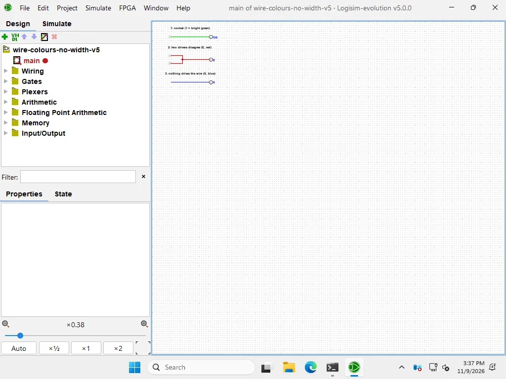
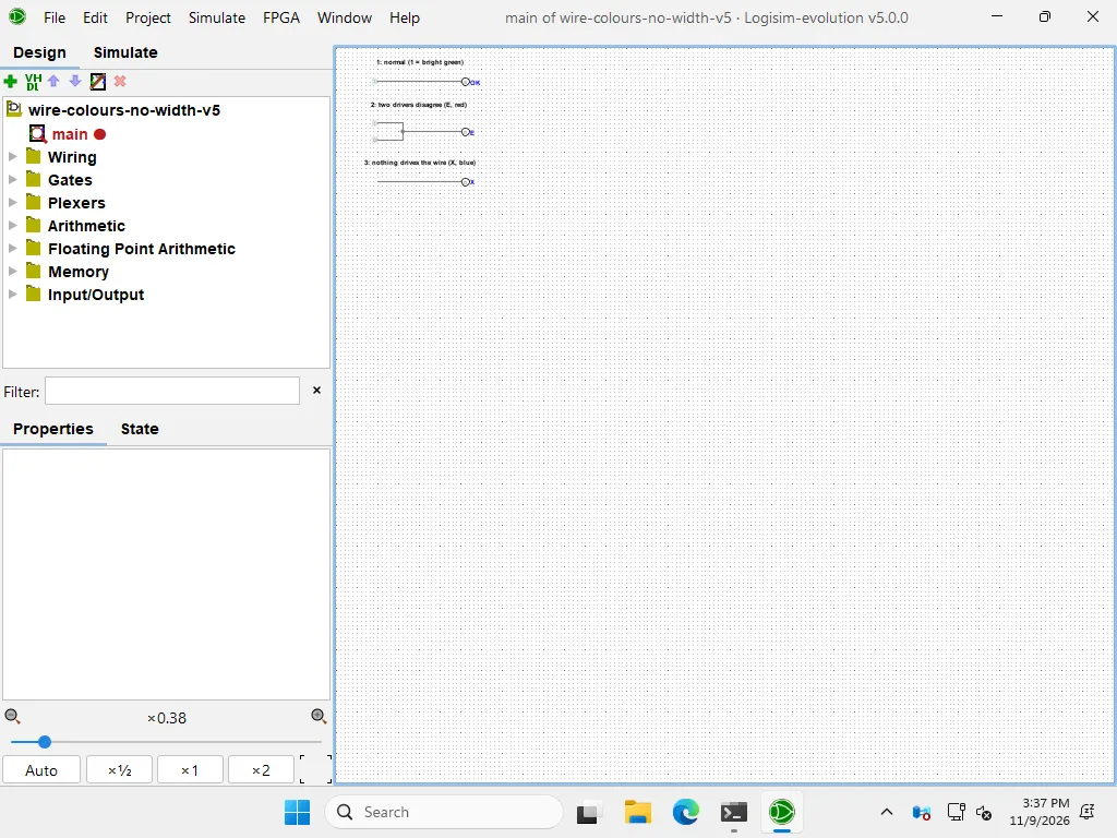 Right after openingAfter one click
Windows Server 2025 desktop on a GitHub runner, 5.0.0 from the MSI.ci-w25-le500-native-v5-before-click-01 · ci-w25-le500-native-v5-after-click-01 Check: After one click on the canvas the wires show their colours again.
You can compare your file with ours, which passes a four-row check in 5.0.0:
Describe this circuit
Components: Input pin A; Input pin B; XOR Gate 1; AND Gate 1; Output pin S; Output pin C.
- Input pin A connects to XOR Gate 1, AND Gate 1 (net A).
- Input pin B connects to XOR Gate 1, AND Gate 1 (net B).
- XOR Gate 1 connects to Output pin S (net S).
- AND Gate 1 connects to Output pin C (net C).
If something looks wrong
| What you see | Cause | Where to look |
|---|---|---|
| A wire is blue, the output reads U | A wire end is not on a port | Blue wire |
| A wire is red, an output reads E | Two outputs drive one wire | Red wire |
| A wire is orange, “Incompatible widths” | Two bit widths meet on one wire | Orange wire |
| Everything is grey after opening any file, yours included | Values are not shown yet | Click the canvas or press Ctrl+R: grey wires |
| Clicking an input does nothing | You are in the Edit tool, which selects instead of toggling | Click the hand (Poke) in the toolbar |
Make it a full adder
A full adder also takes a carry in. Add a third input Cin, a second XOR and AND, and an OR gate: the first XOR gives A⊕B, the second gives the sum S, the two ANDs make the partial carries and the OR combines them into Cout.
Describe this circuit
Components: Input pin A; Input pin B; Input pin Cin; XOR Gate 1; AND Gate 1; XOR Gate 2; AND Gate 2; OR Gate 1; Output pin S; Output pin Cout.
- Input pin A connects to XOR Gate 1, AND Gate 1 (net A).
- Input pin B connects to XOR Gate 1, AND Gate 1 (net B).
- Input pin Cin connects to XOR Gate 2, AND Gate 2 (net Cin).
- XOR Gate 1 connects to XOR Gate 2, AND Gate 2.
- AND Gate 1 connects to OR Gate 1.
- XOR Gate 2 connects to Output pin S (net S).
- AND Gate 2 connects to OR Gate 1.
- OR Gate 1 connects to Output pin Cout (net Cout).
Download circ-tutorial-full-adder.circ and its 8-row test vector. To run the vector, see Test vectors. For the next step, build a 4-bit adder.
Classic 2.7.1 differences you will notice
| Feature | 2.7.1 | 5.0.0 |
|---|---|---|
| Components you can place | 2.7.1: partial57 in 7 libraries | 5.0.0: yes178 in 14 libraries (F23) |
| Opens a file from the other version | 2.7.1: nocannot open 5.0.0 files (F04) | 5.0.0: partialopens 2.7.1 files with a compatibility warning (F02) |
| Menu names for the clock | 2.7.1: untestedTicks Enabled, Tick Once | 5.0.0: yesAuto-Tick Enabled, Manual Tick (F46) |
| Wire colours after opening a file | 2.7.1: untested | 5.0.0: partialgrey until a click or Ctrl+R (F45) |
| Input pin Behavior attribute | 2.7.1: untested | 5.0.0: untestedadded in 4.0 according to upstream, not tested by us |
| Toolbar icons | 2.7.1: untested | 5.0.0: yesas in the shots above |
Next lessons
Download this tutorial as a PDF
A print version of this page, made from the page itself: A4 PDF or US Letter PDF. Logisim-evolution also ships its own tutorial under Help, Tutorial; we do not rehost it.
To see which version made a file and what opens where, read the .circ file page.