What the message means
Logisim recomputes values until nothing changes. If a value is still changing after the project’s iteration limit, it stops. The limit is the option Iterations until oscillation and its default is 1,000 (5.0.0 files record it as simlimit).
Oscillation apparentCanvas status line according to the 5.0.0 strings; see what we saw below
What we saw in 5.0.0 is narrower than the message suggests, so here it is exactly:
- Command line,
--tty table: the output readsEand nothing else is printed (F06, F74). - Test vector: the failing row ends with the word
oscillating, for exampleY = E (expected 0) oscillating(F74). - Window: after one tick of a clock-driven loop the wire turned red and the pin read E. We did not see message text on the canvas in our capture, so we cannot show you the status line (F79). The text
Oscillation apparent
is in the 5.0.0 string table (F73).
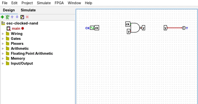
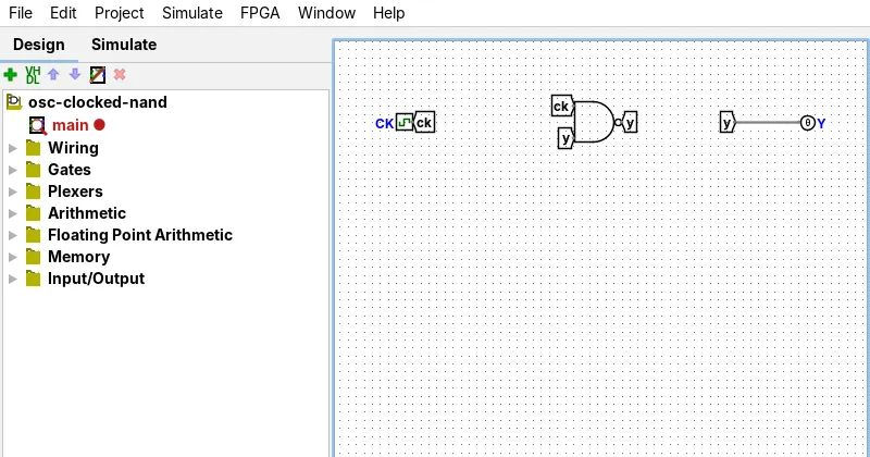
A NOT gate wired to itself is not an oscillation
The smallest loop you can draw, a NOT gate whose output goes straight back to its own input, does not oscillate in 5.0.0. It settles at E: the value is E in the table, the wire is red, and the test vector does not print oscillating (F75, F06). A loop oscillates only when it has a defined value to start from, which is why every example below needs a defined input first.
Describe this circuit
Components: NOT Gate 1; Output pin Q.
- NOT Gate 1 connects to Output pin Q (net Q).
Which cause is yours?
Show all paths
- Does a gate output, or a chain of gates, come back to an input of the same gates without a flip-flop or memory in the path? Yes → Did you build a latch from two NOR or NAND gates that feed each other? Yes → Cause 1: a gate latch
- Does a gate output, or a chain of gates, come back to an input of the same gates without a flip-flop or memory in the path? Yes → Did you build a latch from two NOR or NAND gates that feed each other? No → Is the gate that feeds back the only gate in the loop, wired straight to its own input? Yes, a single gate → Not an oscillation: it settles at E
- Does a gate output, or a chain of gates, come back to an input of the same gates without a flip-flop or memory in the path? Yes → Did you build a latch from two NOR or NAND gates that feed each other? No → Is the gate that feeds back the only gate in the loop, wired straight to its own input? No, several gates → Cause 2: combinational feedback
- Does a gate output, or a chain of gates, come back to an input of the same gates without a flip-flop or memory in the path? No, the loop goes through something else → What is in the loop? A flip-flop with Trigger set to High Level or Low Level → Cause 3: a level-triggered flip-flop
- Does a gate output, or a chain of gates, come back to an input of the same gates without a flip-flop or memory in the path? No, the loop goes through something else → What is in the loop? A ROM or RAM whose data output reaches its own address → Cause 4: a memory loop
- Does a gate output, or a chain of gates, come back to an input of the same gates without a flip-flop or memory in the path? No, the loop goes through something else → What is in the loop? A subcircuit whose output returns to its own input → Cause 5: a loop across subcircuits
- Does a gate output, or a chain of gates, come back to an input of the same gates without a flip-flop or memory in the path? No loop at all, but the circuit is very large → Possibly a false alarm
Five causes we rebuilt and fixed
Every circuit below was checked in Logisim-evolution 5.0.0 with a test vector: the broken one fails on the row shown with the word oscillating, and the fixed one passes (F76).
1. A latch built from gates
Two NOR gates feeding each other make an S-R latch. It works while only one of S and R is 1. Set both to 1, so both outputs drop to 0, and then release both together: each gate now sees two zeros, both outputs rise at the same time, each gate then sees a 1, both fall, and the loop repeats. Every gate in Logisim has the same delay, so the two never get out of step. At power-up with S = R = 0 the table already reads E for both outputs (F76).
| # | S | R | Q | QN |
|---|---|---|---|---|
| 1 | 0 | 1 | 0 | |
| 0 | 0 | 1 | 0 | |
| 1 | 1 | 0 | 0 | |
| 0 | 0 | E | E |
Describe this circuit
Components: Input pin S; Input pin R; NOR Gate 1; NOR Gate 2; Output pin Q; Output pin QN.
- Input pin S connects to NOR Gate 2 (net S, s).
- Input pin R connects to NOR Gate 1 (net R, r).
- NOR Gate 1 connects to NOR Gate 2, Output pin Q (net q, Q).
- NOR Gate 1 connects to NOR Gate 2, Output pin QN (net qn, QN).
Fix.
- Use the built-in D or S-R flip-flop instead of the gate latch (flip-flops).
- If you must build the latch from gates, never release S and R from 1 at the same time.
- Press CtrlR⌘R (⌘R on macOS) to reset the simulation.
Logisim has an option that adds random delays to components, which makes a gate latch settle on its own. Treat it as a teaching aid, not as a fix: a design that only works with random delays is not a design you can trust. We did not test that option.
Describe this circuit
Components: Input pin D; Input pin CLK; D Flip-Flop ff; Output pin Q.
- Input pin D connects to D Flip-Flop ff (net D, d).
- Input pin CLK connects to D Flip-Flop ff (net CLK, clk).
- D Flip-Flop ff connects to Output pin Q (net q, Q).
2. Combinational feedback through gates
Here the output of a gate goes back, perhaps through other gates, to one of its own inputs. NAND(A, Y) driving Y is stable at 1 while A is 0, because a NAND with a 0 input is 1 whatever the other input is. When A becomes 1 the gate becomes an inverter of itself, and the value flips for ever (F75, F76).
Describe this circuit
Components: Input pin A; NAND Gate 1; Output pin Y.
- Input pin A connects to NAND Gate 1 (net A, a).
- NAND Gate 1 connects to Output pin Y (net y, Y).
Fix. Put a register in the feedback path, clocked by the system clock, so that the value changes once per clock edge instead of in a loop. If you wanted a state that holds, use a flip-flop for it.
Describe this circuit
Components: Input pin A; Input pin CLK; NAND Gate 1; D Flip-Flop ff; Output pin Y.
- Input pin A connects to NAND Gate 1 (net A, a).
- Input pin CLK connects to D Flip-Flop ff (net CLK, clk).
- NAND Gate 1 connects to D Flip-Flop ff (net d).
- NAND Gate 1 connects to D Flip-Flop ff, Output pin Y (net y, Y).
3. A level-triggered flip-flop that toggles
We started this page expecting a clock wired into its own logic to oscillate. It did not (see below). What did oscillate is a flip-flop whose Trigger attribute is set to High Level, with its input wired to its own complement. While the clock is 1 the flip-flop is transparent, so it keeps copying the opposite of what it just stored. With the clock at 0 the output is 0; at 1 it is E (F76).
Describe this circuit
Components: Input pin CLK; D Flip-Flop ff; Output pin Q.
- Input pin CLK connects to D Flip-Flop ff (net CLK, clk).
- D Flip-Flop ff connects to Output pin Q (net q, Q).
Fix. Set Trigger to Rising Edge or Falling Edge in the Properties panel. The same wiring then toggles once per clock cycle.
Describe this circuit
Components: Input pin CLK; D Flip-Flop ff; Output pin Q.
- Input pin CLK connects to D Flip-Flop ff (net CLK, clk).
- D Flip-Flop ff connects to Output pin Q (net q, Q).
4. A memory output looped to its own address
A ROM answers every address with a value. If that value is wired back to the ROM’s address through a multiplexer that lets it run, each answer becomes the next address, and the circuit moves through values without end. Our ROM holds the next number at every address, and the multiplexer first loads a starting address and then lets the loop run (F76). A RAM wired the same way behaves like a ROM with the contents you wrote into it; we tested a ROM only.
Describe this circuit
Components: Input pin START; Input pin RUN; Multiplexer 1; ROM prog; Output pin Q.
- Input pin START connects to Multiplexer 1 (net START, st), 8 bits wide.
- Input pin RUN connects to Multiplexer 1 (net RUN, run).
- Multiplexer 1 connects to ROM prog, Output pin Q (net d, Q), 8 bits wide.
- Multiplexer 1 connects to ROM prog, 8 bits wide.
Fix. Put a register in the address path, so that the address changes once per clock edge (see RAM and ROM).
Describe this circuit
Components: Input pin START; Input pin RUN; Input pin CLK; Multiplexer 1; Register stage; ROM prog; Output pin Q.
- Input pin START connects to Multiplexer 1 (net START, st), 8 bits wide.
- Input pin RUN connects to Multiplexer 1 (net RUN, run).
- Input pin CLK connects to Register stage (net CLK, clk).
- Multiplexer 1 connects to Register stage (net rq), 8 bits wide.
- Multiplexer 1 connects to ROM prog, 8 bits wide.
- Register stage connects to ROM prog, Output pin Q (net d, Q), 8 bits wide.
5. A loop that crosses subcircuits
A subcircuit can hide half of a loop. In our circuit the subcircuit holds a NAND gate; in the parent circuit its output is wired back to its own second input, just like cause 2. Nothing inside the subcircuit looks wrong. The red may show only on the wire in the parent, or in both places (F76). To find such a loop, follow the red wires, and open each subcircuit (Subcircuits).
Describe this circuit
Components: Input pin EN; nandcell u1; Output pin Y.
- Input pin EN connects to nandcell u1 (net EN, en).
- nandcell u1 connects to Output pin Y (net y, Y).
Fix. Put a register in the parent, in the path from the subcircuit’s output back to its input.
Describe this circuit
Components: Input pin EN; Input pin CLK; nandcell u1; D Flip-Flop ff; Output pin Y.
- Input pin EN connects to nandcell u1 (net EN, en).
- Input pin CLK connects to D Flip-Flop ff (net CLK, clk).
- nandcell u1 connects to D Flip-Flop ff, Output pin Y (net y, Y).
- nandcell u1 connects to D Flip-Flop ff (net x).
What did not oscillate
Two wirings that many guides describe as oscillating did not, in our tests:
- A single NOT gate (or one gate inside a subcircuit) wired to its own input settles at E (F75).
- A D flip-flop whose clock was taken from its own inverted output stayed at 0 in the command-line table (F77).
We did not test a counter or register whose output feeds its own clear, so this page makes no claim about it.
When it is a false alarm: raising the limit
The iteration limit counts propagation steps, and a long path of gates takes one step per gate. In our test a line of NOT gates from one pin to one output settled with the default limit of 1,000 for 980 and 990 gates. With 1,000, 1,010 and 1,100 gates the output read E for both input values, although nothing loops (F78). With the limit raised to 3,000, the 1,100-gate chain followed its input.
| # | A | Y with limit 1,000 | Y with limit 3,000 |
|---|---|---|---|
| 0 | E | 0 | |
| 1 | E | 1 |
To change it, choose Project, Options and open the Simulation tab; the setting is called Iterations until oscillation. Raise it only when you know the circuit is stable, for example a very long chain, and only as far as you need. It is stored in the file.
Both chains are too wide to draw here. Download the chain with the default limit and the chain with the limit raised to 3,000.
After the fix: get the simulation running again
- Press CtrlR⌘R (⌘R on macOS) (Simulate, Reset Simulation). The loop stays in the error state until you reset.
- Check that Auto-Propagate is on (Simulate menu, Ctrl+E in 5.0.0, F46).
- If you use a clock, check that ticks are enabled. See Clock and simulation.
How to find the loop in a big circuit
- Follow the red wires back to a gate output that returns to an input of the same chain. Red wires and E are explained in wire colours.
- Use Single-Step Propagation (Ctrl+I) to watch values move one step at a time.
- Split the design into subcircuits and test each with a test vector. A failing row ends with the word oscillating when the cause is a loop (F74).
- Open the timing diagram to see a value toggle (timing diagram).
Why real hardware and Logisim differ
Real gates have slightly different delays, so many loops settle on one state. In Logisim every component has a fixed delay inside one global schedule, which is why symmetric loops such as a NOR latch flip in lockstep. The Logisim-evolution documentation describes this limit and the option for random delays.
Digital, another simulator, treats some loops differently. We have not tested Digital. See Logisim compared with Digital.
Classic 2.7.1
| Feature | 2.7.1 | 5.0.0 |
|---|---|---|
| Iteration limit stored in the file as | 2.7.1: untestedsim_limit in our classic files | 5.0.0: yessimlimit in 5.0.0 files |
| NOR latch released from S = R = 1 | 2.7.1: untested | 5.0.0: yesoscillates (F76) |
| Single NOT gate wired to itself | 2.7.1: untested | 5.0.0: yessettles at E (F75) |
Cells say untested where we did not run 2.7.1.
Downloads
Each pair has a broken and a fixed file. The broken files are checked to fail with the word oscillating on the rows named in their descriptions; the fixed files pass a test vector. All are CC BY 4.0 and open in the .circ Viewer.
| Cause | Broken | Fixed |
|---|---|---|
| NOR latch | sr-latch-broken | sr-latch-fixed |
| Gate feedback | gate-feedback-broken | gate-feedback-fixed |
| Level-triggered flip-flop | level-trigger-broken | level-trigger-fixed |
| Memory loop | memory-loop-broken | memory-loop-fixed |
| Subcircuit loop | subcircuit-loop-broken | subcircuit-loop-fixed |
| Single gate (settles at E) | not-loop |